7. Memory Map and Bus Interfaces
1. Memory Map in ARM Cortex-M
What is a Memory Map?
In ARM Cortex-M microcontrollers like the STM32 series, a memory map defines how the processor's address space is partitioned and what each address space corresponds to. The memory map consists of regions designated for specific functions—like Flash memory for code, RAM for data storage, and peripheral registers for controlling hardware components. Memory maps provide a structured way to access these resources.
To learn more about memory map, refer to the ARM Cortex-M4 Generic User Guide, Section 2.2 ("Memory model"):
Memory Types
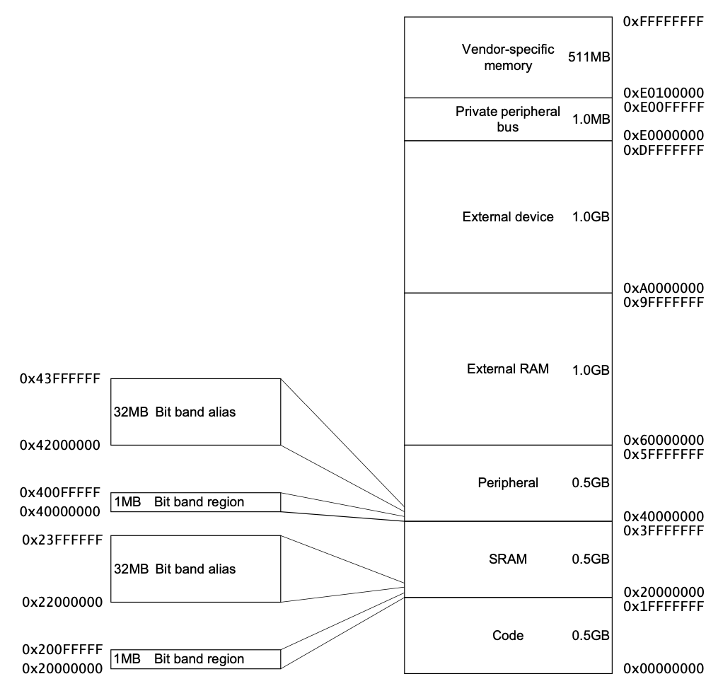
| Memory Type | Purpose/Content | Address Range (Typical) | Size (Typical) | Underlying Hardware | eXecute Never (XN) |
|---|---|---|---|---|---|
| Code Memory (Flash) | Program code, constants | 0x00000000 - 0x1FFFFFFF | 0.5 GB | Flash memory | No |
| SRAM | Data storage, stack, heap | 0x20000000 - 0x3FFFFFFF | 0.5 GB | Static RAM | No |
| Peripheral | Registers for onboard peripherals | 0x40000000 - 0x5FFFFFFF | 0.5 GB | Peripheral registers | Yes |
| External RAM | Data storage | 0x60000000 - 0x9FFFFFFF | 1.0 GB | External RAM | Optional |
| External Device | Memory-mapped devices | 0xA0000000 - 0xDFFFFFFF | 1.0 GB | External I/O | Yes |
| Private Peripheral Bus | Cortex-M core peripherals | 0xE000E000 - 0xE00FFFFF | 1 MB | Special-purpose logic | Yes |
| Vendor-Specific Memory | OEM custom memory regions | 0xE01000000 - 0xFFFFFFFF | Up to 511 MB | Custom | Optional |
- eXecute Never (XN) means that code cannot be executed from this memory region. This is a security feature that prevents code injection attacks.
Address Range and Size
A 32-bit ARM Cortex-M processor has a 32-bit address space, meaning it can address unique locations. That translates to 4GB of addressable memory. However, not all addresses are guaranteed to be valid; attempting to access an invalid address usually leads to a fault or undefined behavior.
How Many GB Can Be Addressed?
A 32-bit ARM Cortex-M can technically specify up to 4GB of addressable space. However, most MCUs, including the STM32 series, don't come anywhere near that limit. They're designed for embedded applications where memory requirements are far less.
What if There's More Than 4GB?
While exceeding 4GB is not an issue for STM32 MCUs due to their design constraints, there are techniques to address more than 4GB in other types of systems. These include bank switching, using a Memory Management Unit (MMU), extended addressing modes, and segmentation. However, these methods are generally not applicable to ARM Cortex-M MCUs.
Are All Address Regions the Same?
Even though you access different types of memory and peripherals using addresses, these addresses don't all point to the same kind of hardware. For example, addresses in the Flash region point to non-volatile memory that holds your program code, while addresses in the RAM region point to volatile memory used for data storage during program execution.
2. Bus Protocols and Interfaces
A bus is a set of electrical conductors that enable data transfer between different components in a computer or microcontroller. Think of it as the data "highway" within the device.
Bus Protocols
Bus protocols establish the rules for communication between devices connected to the bus. These rules cover initiating and terminating data transfers, packaging data, and addressing.
AMBA Specification by ARM Cortex-Mx
ARM's Advanced Microcontroller Bus Architecture (AMBA) specification outlines various supported bus protocols for ARM Cortex-Mx series:
-
Advanced High-performance Bus Lite (AHB Lite): This is often considered the "main bus" as it is designed for high-speed communication between the CPU, on-chip memory, and on-chip peripherals. AHB Lite is capable of high-throughput data transfers and is crucial for real-time applications.
-
Advanced Peripheral Bus (APB): APB is generally slower and is meant for peripherals that don't require high-speed operation. The APB can be accessed through an AHB-APB bridge. This bus is ideal for less time-sensitive operations like reading sensor data or simple I/O operations.
STM32F446xx Memory Map and Bus Configuration
Referencing the datasheet of STM32F446xx, you'll notice it has a detailed memory map:
Within this architecture, there are several buses with different characteristics:
-
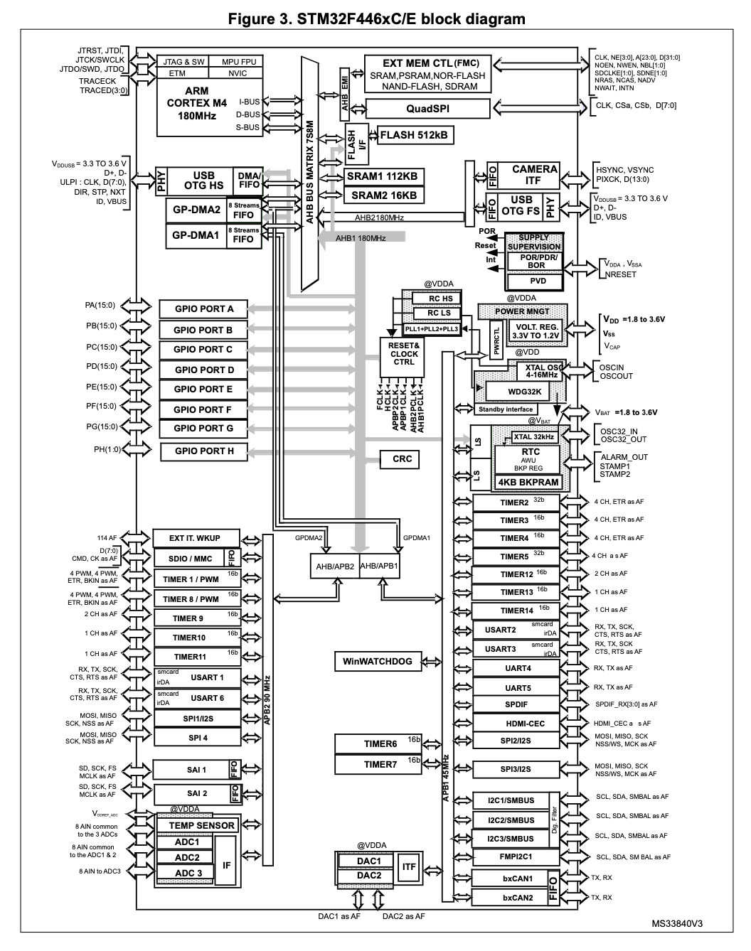
AHB1: Commonly called the "main bus," it operates at a speed of 180MHz and handles high-throughput data transfers.
-
AHB2: Similar to AHB1 but may be designated for specific purposes, such as connections to specific, high-speed peripherals like USB OTG HS, camera interface, or even specialized memory blocks. Also operates at 180MHz.
-
AHB3: AHB3 bus is sometimes referred to as the AHB-EMI (External Memory Interface). This bus is specifically designed for connecting the microcontroller to external memory devices. This is especially useful for applications requiring larger memory storage or high-speed read/write operations that can't be met by the internal memory.
-
APB1: Operates at a slower 45MHz and is used for peripherals that don't require high-speed data transfers (e.g., UART, I2C, timers, etc.).
-
APB2: Slightly faster than APB1, operating at 90MHz. It's used for peripherals that need a bit more speed than those connected to APB1 but don't require the full speed of an AHB (e.g., SPI, ADC, certain timers, etc.)
Bus Interfaces
A bus interface is the actual hardware that hooks a component up to a bus. It makes sure that component can "speak the language" of a specific bus protocol. It's like the 'connector' that translates the component's operations into signals that can travel over the bus.
ARM Cortex-Mx Processor Interfaces
ARM Cortex-Mx microcontrollers come with several AHB interfaces for various functions:
-
PPB (Private Peripheral Bus): This interface provides a connection to private peripherals of the microcontroller, often those used for system configuration and control.
-
System Bus (S-Bus): This interface handles any read/write access to SRAM, Peripheral registers, External RAM, External Device (I/O), and possibly also vendor-specific memory areas.
-
D-Bus: This is used for data accesses, particularly those that read from or write to the code memory.
-
I-Bus: This interface is responsible for fetching instructions and vector tables specifically from code memory.
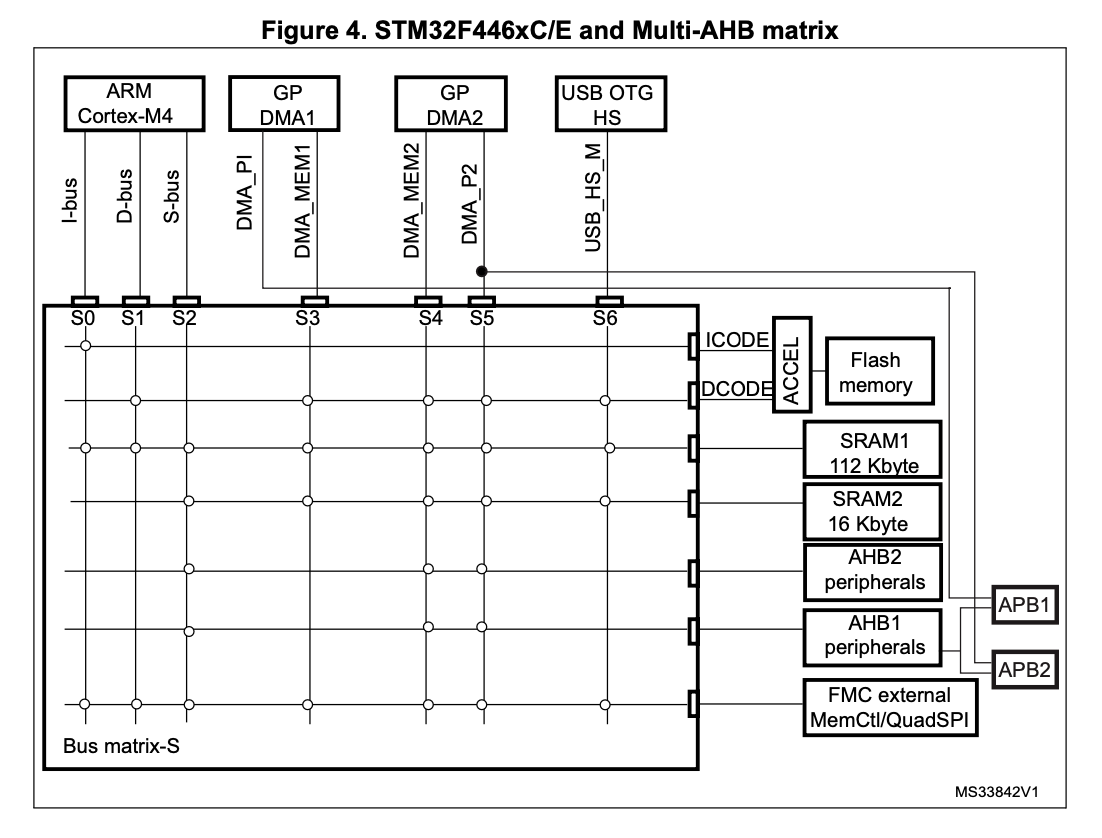
Bus Matrix
A bus matrix is like a high-speed road network that connects various parts of your system. It's an arrangement of multiple buses that lets you move data more flexibly between different peripherals, memory locations, and processors. The idea is to cut down on data traffic jams and make it possible for different parts of the system to operate in parallel.
In the context of the STM32F446xx, the 32-bit multi-AHB bus matrix links all the masters—like the CPU, DMAs, and USB HS—to slaves like Flash memory, RAM, QuadSPI, FMC, and AHB and APB peripherals. This setup helps the system run smoothly, even when several high-speed peripherals are operating at the same time.
3. Bit Banding
Working with individual bits within a memory location often requires reading the whole byte, modifying the bits you're interested in, and then writing the entire byte back. Traditional approaches involve using bitwise operations, like OR or AND, combined with masking and shifting. While these methods work, they can be computationally intensive and may result in non-atomic operations.
What is Bit Banding?
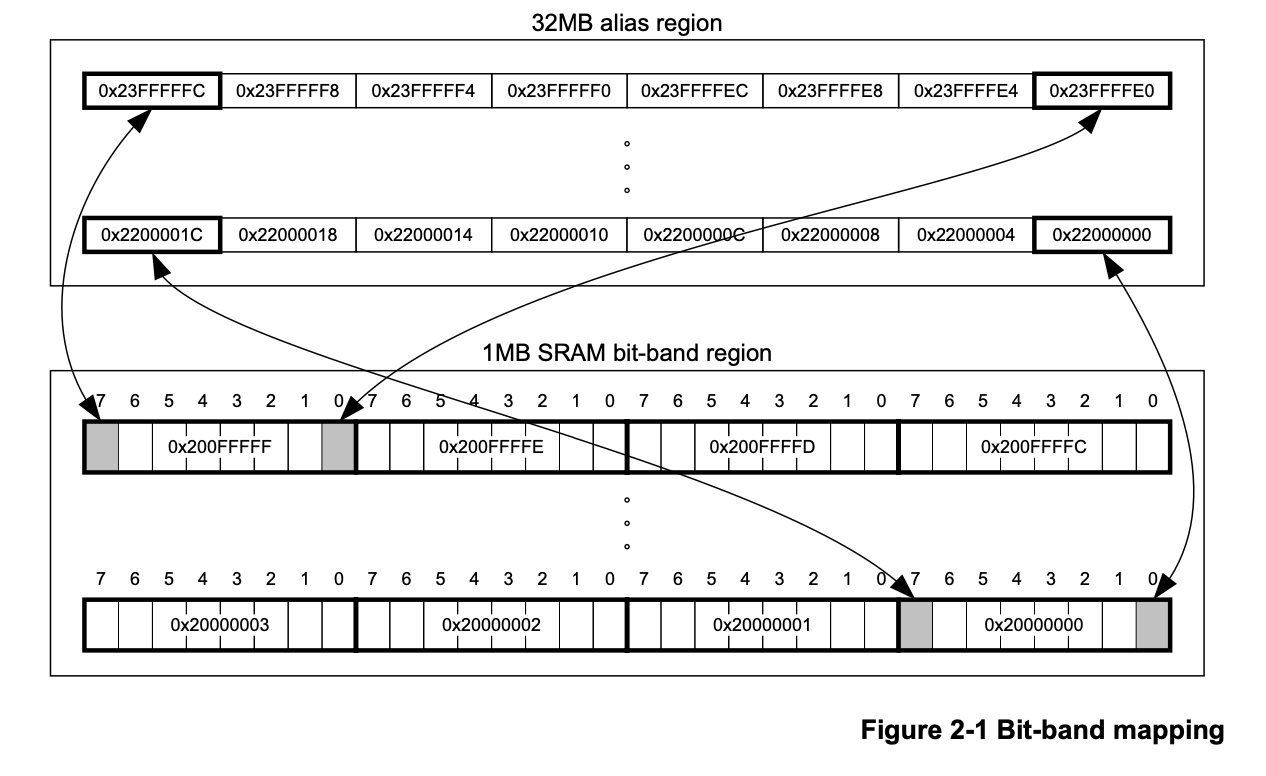
Bit banding offers a more efficient way to read and write individual bits in a memory location. It maps a complete word of memory onto a single bit in a designated bit-band region. Essentially, each bit in the bit-band alias region corresponds to a specific bit in the original memory location.
Where is Bit Banding Supported?
Bit banding is not universally supported across all ARM Cortex-M processors. On the ARM Cortex-M4, bit banding is supported for specific regions of SRAM and peripheral memory. These bit-band regions occupy the lowest 1MB of the SRAM and peripheral memory regions.
How Does it Work?
Accesses to the 32MB SRAM alias region map onto the 1MB SRAM bit-band region. Similarly, accesses to the 32MB peripheral alias region map onto the 1MB peripheral bit-band region. Each word (32-bits) in the alias region directly relates to a single bit in the bit-band region.
Why Use Bit Banding?
-
Atomic Operations: Bit banding ensures that read-modify-write operations are atomic. This is critical in real-time systems where interrupts could jeopardize the integrity of regular bit-wise operations.
-
Code Efficiency: Bit banding simplifies the code needed for bit manipulation, making it easier to read and maintain.
-
Performance: Directly accessing individual bits can be faster than traditional methods, especially when multiple bit manipulations are required in quick succession.
Further Reading
For a deep dive into the specifics, the ARM Cortex-M4 Generic User Guide, Section 2.2.5 ("Optional bit-banding"), is an excellent resource.
This feature can be particularly handy in applications that require precise, real-time control over hardware settings or any other scenario where individual bit manipulation is a common task.
Calculating Bit Band Addresses
In SRAM, you have the original "word" addresses where each address points to a 32-bit word. On the other hand, you have a separate "alias" region. Each address in this alias region essentially maps to a specific bit in a word at the original address. This enables you to access individual bits as if they were full 32-bit words, making bit-level operations more straightforward and potentially more efficient.
The formula to calculate the bit-band alias address is given by:
- Bit-band base address: This is the starting address of the bit-band region.
- Word address: This is the address of the target bit in the non-aliased, 32-bit word.
- Alias base address: This is the starting address of the alias region.
- Bit number: This is the bit position (0-31) in the word.
The multiplication by 32 is because each word in the alias region maps to a unique bit in the bit-band region, and a word is 4 bytes. So, 8 bits (1 byte) × 4 = 32.
The multiplication by 4 for the bit number is because each bit in the bit-band region is represented by a word (4 bytes) in the alias region.
This formula lets you directly read or write to a specific bit while treating it as a regular 32-bit variable, thanks to the bit-band alias.
The base addresses for ARM Cortex-M4 are as follows (see the very first figure in this section):
| Region | Bit-band base address | Alias base address |
|---|---|---|
| SRAM | 0x20000000 | 0x22000000 |
| Peripheral | 0x40000000 | 0x42000000 |
Example
Question: Find the 7-th bit position of the memory address 0x2000_0200 using its bit-band alias address.
Answer:
We can achieve the same result using the following C code:
#include <stdint.h>

// Constants for bit-banding
const uint32_t AliasBase = 0x22000000U;
const uint32_t BitbandBase = 0x20000000U;

// Function to calculate bit-band alias address
uint8_t* getBitbandAliasAddress(uint32_t originalAddr, uint8_t bitPosition) {
    return (uint8_t*)(AliasBase + (32 * (originalAddr - BitbandBase)) + (bitPosition * 4));
}

int main(void) {
    // Initialize a byte at address 0x20000200 with 0xFF
    uint8_t* bytePtr = (uint8_t*)0x20000200;
    *bytePtr = 0xFF;

    // Clear the 7th bit using normal bitwise operations
    *bytePtr &= ~(1 << 7);

    // Reset the value to 0xFF
    *bytePtr = 0xFF;

    // Clear the 7th bit using bit-banding
    uint8_t* aliasAddr = getBitbandAliasAddress(0x20000200, 7);
    *aliasAddr = 0;

    // Endless loop
    for (;;) {}
}
Note that we are casting the addresses to uint8_t* because we want to access individual bytes. If we were working with 32-bit words, we would cast to uint32_t* instead.